Having grown up with the Commodore 64 in the eighties, I was always somewhat connected to this charming old school computer, but for 30 years or so I totally lost interest in the real hardware, was satisfied with emulators and got rid of my disk drive and all the physical disks and tapes. In late 2019, for some nostalgic reason, I felt the urge to repair my good old "bread bin", which restored my interest in the actual hardware. Now my old breadbin C64 has an older "long board" revision 250407 which doesn't have the best picture quality. I tried to improve that by exchanging the modulator, the video chip (VIC) and so on, but to be frank, I reached a limit there due to the board design and being limited to the old NMOS VIC. Besides, the old power supply is clumsy and most extensions like a dual-SID (sound IC) support force you to solder cables inside the computer.
Now, there are some commercial offerings to overcome all these limitation, namely the iComp C64 Reloaded MK2 and the Ultimate 64. Both are very interesting designs, but didn't really satisfy my desire for an optimized classical C64 board. The Reloaded MK2 replaced more or less everything but the main ICs (CPU, VIC, SID, CIAs) with SMD components, so it's not really usable as a reference system to check a PLA or RAM. The Ultimate 64 is an FPGA design which makes a lot of fascinating things possible, but it only allows to use original SIDs and is obviously not usable as a reference board. There's also a "64 Tuning Board" but it lacks some features like the 9V AC supply on the user port and it's based on the later "short board" revisions without a classic PLA - which was totally reverse engineered many years ago, so there are lots of cheap replacements available.
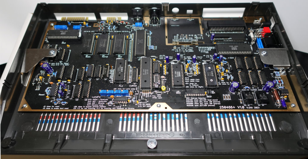
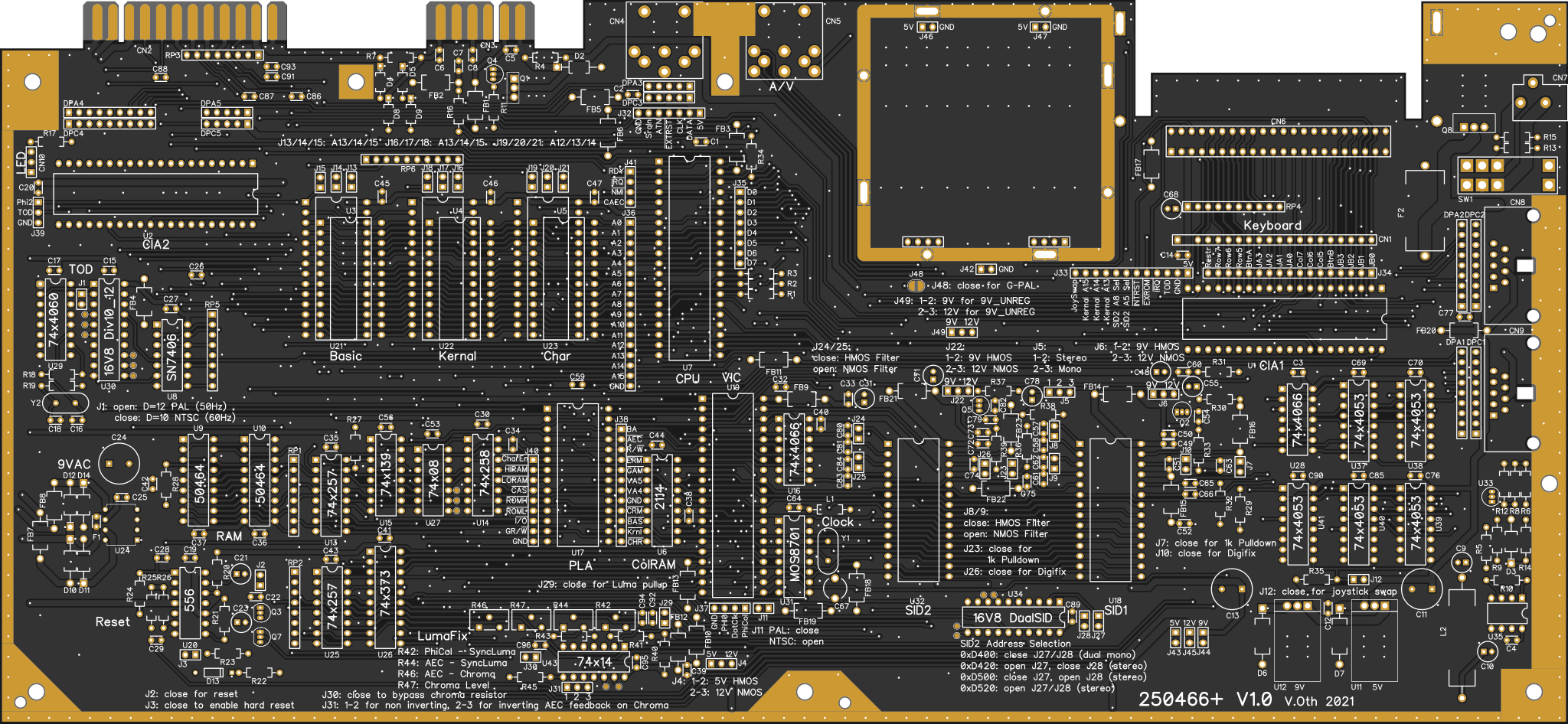
I learned that the board revision 250466 is something quite a few people are considering the best board revision as it was last the "long board" with the original NMOS chipset with separate PLA and three ROMs but also featured some improvements over the older boards, like using only two 32kBit RAMs (instead of eight 8kBit RAMs) and having a much simplified clock circuit. So I wondered if the design of the 250466 couldn't be improved to get an old school C64 mainboard being able to use all the ICs from an original board but also offering some features that usually need modifications. I began working on this in April 2021 when I also started the according thread in the German Forum64 and finally finished building and testing V1.0 in October 2021.
The main design is taken over from the board revision as shown in the 250466 C64C service manual. I did a few changes here and there, e.g. added additional protection diodes and EMC capacitors from the 250469 boards. I also added additional protection diodes which didn't exist in the 250469 boards (even though there are footprints for protection diodes on the 250469 boards, they never were placed).
The reverse current protection is realized through the body diode of the N-FET Q8 and the FUSE F2.
The over-voltage protection is implemented using a voltage reference TLE431 and a comparator TLC3702 (with push/pull output) which triggers the FET to blow the fuse. There is a 15V Zener diode in the supply of the comparator to protect both, the comparator and the FET's gate from higher voltages.
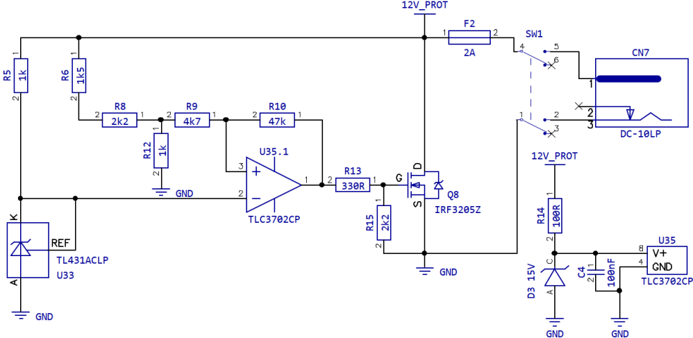
If the voltage rises above ~13.3V, the output of the comparator jumps from ground to its supply voltage. This triggers the FET which creates a deliberate short circuit to ground to blow the fuse.
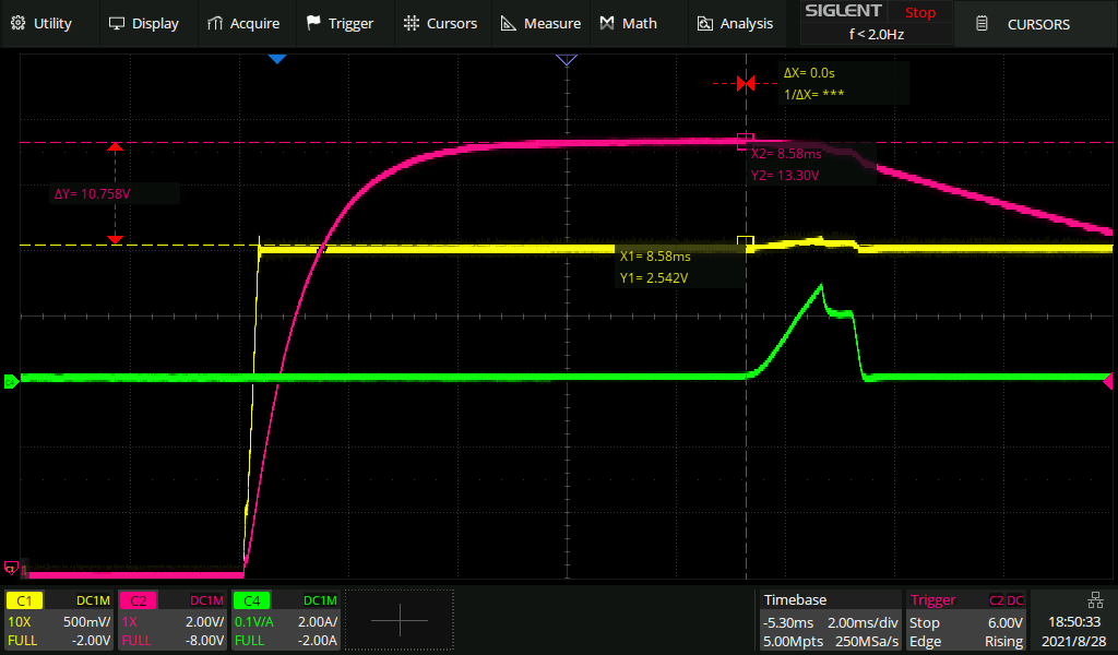
C1/yellow is the voltage at the cathode of the TL431, C2/red is the supply voltage, C3/green is the current. Note that I used the electronic fuse of my power supply here, set to 2A, so the current drop is caused by the fuse kicking in.
Thanks to Ruudi aka ChipMonk from Forum64 for supporting me with suggestions and constructive criticism.
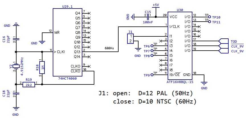
Since the 50/60Hz timer TOD (time of day) is derived form the AC supply in the original boards, I had to come up with a replacement circuit. At first I wanted to use only discrete logic ICs to create it, but to reduce complexity and to be able to add special features, I decided to use a programmable logic device (ATF16V8). The 74HCT4060 is four stage binary counter with oscillator. Together with the 4.9152MHz crystal and a fixed divider of 8192 (1<<13), it creates a 600Hz signal - which however isn't symmetrical. Depending on the jumper setting, the logic programmed into the PLD divides this frequency by 10 (NTSC) or 12 (PAL) and creates a symmetrical 60Hz/50HZ TOD signal.
The other two outputs are used to create the 9V AC using the following circuit:
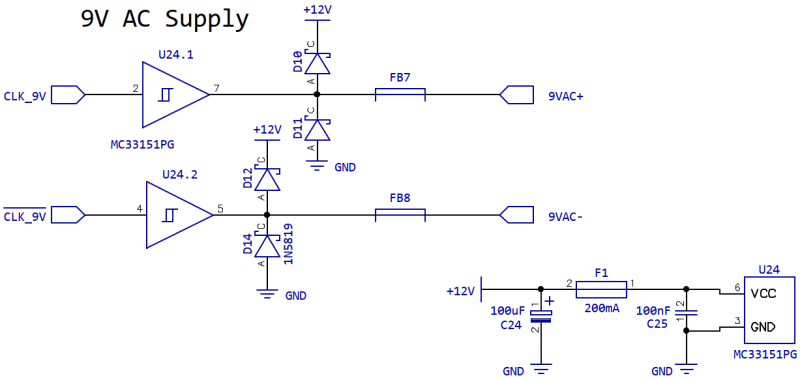
In a nutshell, the High dual MOSFET Driver MC33151 is used to switch the 9VAC+ and 9VAC- outputs alternatingly to either 12V or GND where the inverted control signal /CLK_9V is used to create an inverted switching on 9VAC- compared to 9VAC+.
Now, directly switching the 12V from one output to the other would theoretically create a 12V RMS (root mean square) signal. Also directly switching the 12V from one side to the other would create a steep transient. So a little trick is used to make the signal look a bit more like a sine and also get closer to a 9V RMS. Using the PLD, an delay is added. So instead of switching 12V directly from one side to the other, both outputs are switched to ground during the transition.
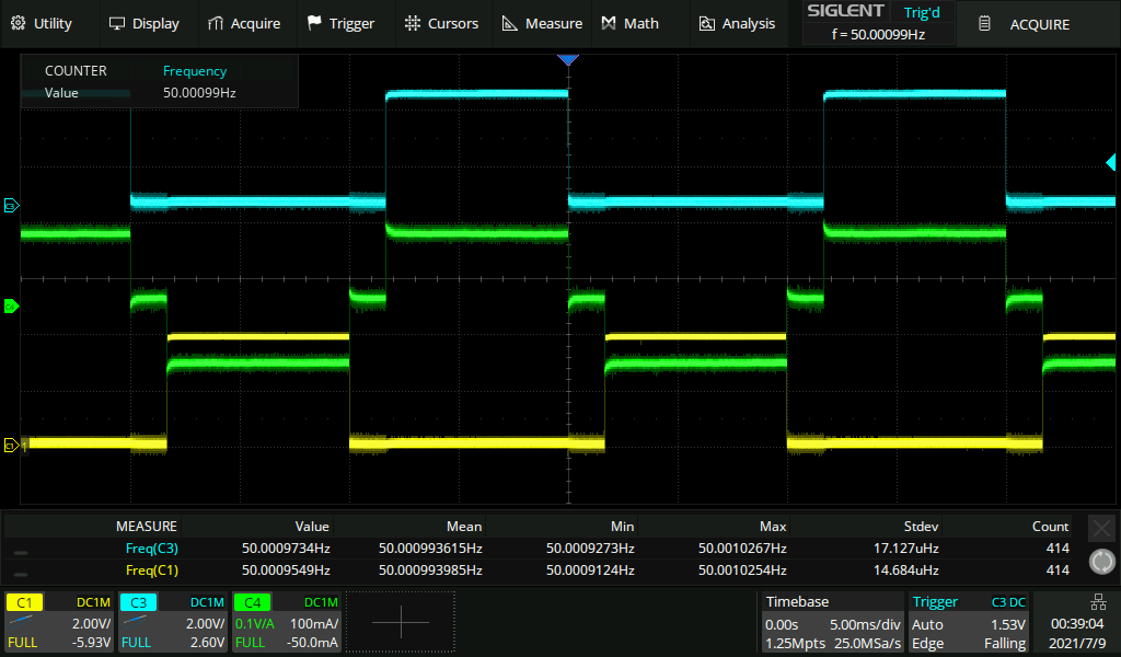
C1/yellow and C3 (cyan) are the both sides of the 9VAC output and C4/green is the current through a 68Ohm load.
To test that this works with voltage multipliers used e.g. in user port EPROM programmers, I recreated the voltage multiplier stage of a Dela EPROMMER II and connected it to this "9VAC" output.
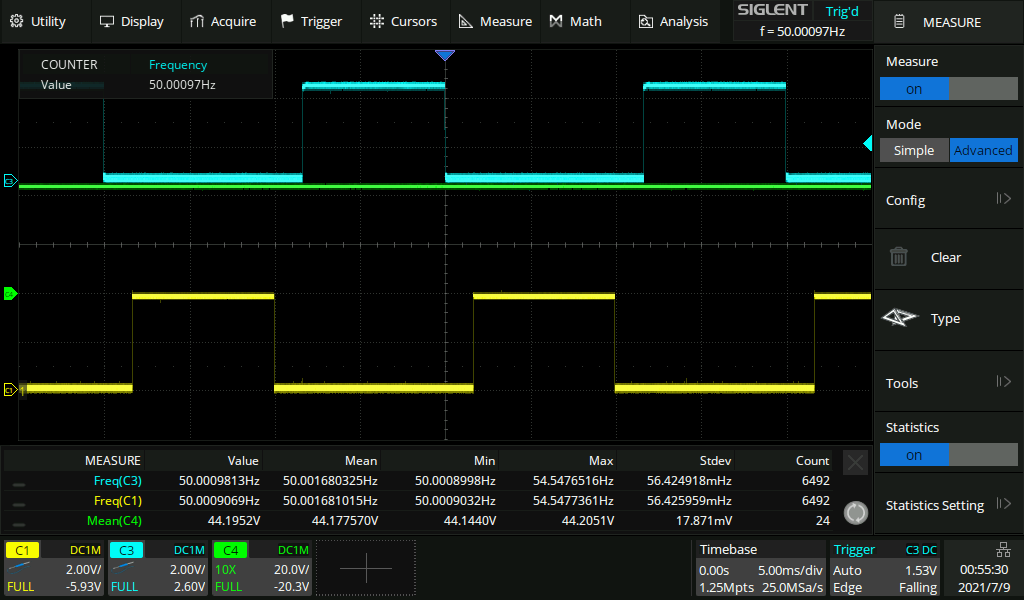
C3/green is the voltage at the multiplier output which is 42.2V. With a 2k load on the voltage multiplier (resulting in a current of about 20mA), the voltage drops to ~37.5V which fits the expectations and matches the behavior of the original circuit on a real C64.
Thanks to Wiesel from Forum64 for valuable hints and suggestions.
My aim for DualSID support was to allow to select the typically used addresses 0xD020 and 0xD500 for the 2nd SID by accessing the address lines A5 and A8. Using two address selection jumpers, this also allows to select 0xD400 and 0xD520. While 0xD520 is just another uncommon address that can be used for the 2nd SID, I figured that 0xD400 (i.e. the default address) could be used for a dual mono mode. I.e. both SIDs play the same sound/song, but e.g. by using a NMOS SID as first SID and a HMOS SID
as 2nd SID, this could create a semi-stereo sound for normal
(mono) games. By comparing the address lines A5 and A8 with the selected values A5_SEL and A8_SEL, the SID chipselect can be either directed to the first or 2nd SID. For dual-mono-mode, the CS is just passed through, but there is a catch: when reading registers from the SID in dual-mono-mode (e.g. PotX/Y values), only the first SID must respond. Therefore the R/W line has to be monitored and the chip select for the 2nd SID has to be suppressed in case of a read access in dual-mono mode.
Again, I initially wanted to implement this using discrete logic ICs, but to reduce the IC count and allow for more flexibility, I decided to use a 2nd programmable logic device (ATF16V8).
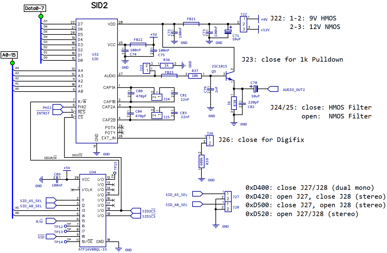
Note that passing the R/W line for the 2nd SID through the PLD was a cautionary measure. In the end, I didn't use it and the signal is just passed through.
On most C64s, there is a certain amount of crosstalk between the AEC and Phi Color signals and the chroma/luminance signals created by the VIC. Most notably, there are lighter/darker vertical bars visible on the screen.
Therefore a somewhat typical lumafix/stripefix design was integrated on the mainboard. The functionality can be completely disabled by not placing U43 (70HCT14) and closing the jumper J30.
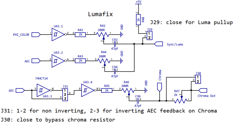
Note that the Lumafix design was originally developed by ikary_01 from forum64.de, e5frog from lemon64.com and other folks. I just took over the open design into my board.
While most games use the 2nd joystick port, there are quite a few which only support the 1st port. So when playing games on a C64, it happens quite a lot that you need change the joystick from one port to the other. So even back in the days, there were joystick port switches offered and there still are quite a few offerings available. Most of them have to be plugged into the joystick ports and are actually quite large, so they are clumsy and cause mechanical stress. So I decided to include a joystick
port switch in my
design. It's a straight forward approach using triple 2-channel analog multiplexers/demultiplexers 74HCT4053. There seven lines to swap (Joy1/2/3/4, JoyBtn, PotX/Y) for two ports and each 74HCT4053 can handle three lines, so there are five 74HCT4053 needed.
All the selects lines (S1/S2/S3) on each 74HTC4053 are connected and pulled up by default which selects the default joystick port layout (nY1). When pulling down this control signal by either closing J12 or driving JOYSWAP to ground, the alternative (swapped) layout is selected (nY0).
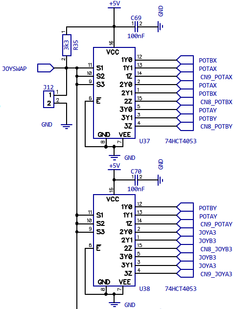
Again, this is a commonly used design used in a similar way before for external switches.
Thanks to ClausS from Forum64 for pointing out a blatant mistake in my original schematics.
There are a lot of jumpers on the board, so this is supposed to give an overview
| J1 | This is the TOD PAL/NTSC selection. Leave open for PAL (50Hz), close for NTSC (60Hz). Note that this will only affect the TOD frequency used by the CIAs |
| J2 | Reset switch. Close (for a short time) to create a reset |
| J3 | Hard reset. Close to create a hard reset with J2. Hard resets means that the module identifier "CBM80" at 0x8004 is not recognized to also work with software that uses this ID to protect itself against a normal reset |
| J4 | Select VIC voltage supply. Close 1-2 for 5V/HMOS, close 2-3 for 12V/NMOS. Don't apply 12V to a HMOS VIC!!! |
| J5 | Selects which SID's output is connected to Pin 7 of the AV connector. Close 1-2 to connect the 2nd SID (stereo). Close 2-3 to connect the 1st SID (mono). |
| J6 | Voltage selection for SID1. Close 1-2 for 9V/HMOS, close 2-3 for 12V/NMOS. Don't apply 12V to a HMOS SID!!! |
| J7 | Close for 1k pulldown in SID output filter, else leave open. Note that this pulldown is only needed for the NMOS (12V) SID. So, close for NMOS SID and open for HMOS SID. |
| J8/9 | SID filter capacitor selection. Close for HMOS Filter, open for NMOS filter |
| J10 | SID "Digifx" for too silent samples on HMOS VIC. Close to activate Digifix (don't use on NMOS SID) |
| J11 | PAL/NTSC selection for clock generator MOS8701. Close for PAL, open for NTSC. |
| J12 | Joystick swap: close to swap all signal lines of both joystick ports. Leave open for normal joystick port assignment |
| J13/14/15 | Selects the address lines A13/14/15 for the Basic (E)EPROM. The lines are pulled up (1) by default and closing a jumper selects a 0 for the according address line. Allows to select 1 of 8 Basic ROMs. |
| J16/17/18 | Selects the address lines A13/14/15 for the Kernal (E)EPROM. The lines are pulled up (1) by default and closing a jumper selects a 0 for the according address line. Allows to select 1 of 8 Kernal ROMs. |
| J19/20/21 | Selects the address lines A12/13/14 for the Character (E)EPROM. The lines are pulled up (1) by default and closing a jumper selects a 0 for the according address line. Allows to select 1 of 8 Character ROMs. |
| J22 | Voltage selection for SID2. Close 1-2 for 9V/HMOS, close 2-3 for 12V/NMOS. Don't apply 12V to a HMOS SID!!! |
| J23 | Close for 1k pulldown in SID2 output filter, else leave open. Note that this pulldown is only needed for the NMOS (12V) SID. So, close for NMOS SID and open for HMOS SID. |
| J24/25 | SID2 filter capacitor selection. Close for HMOS Filter, open for NMOS filter |
| J26 | SID2 "Digifx" for too silent samples on HMOS VIC. Close to activate Digifix (don't use on NMOS SID) |
| J27/28 | SID2 address selection for A5 (J27) and A6 (J28). 0xD400: close J27/J28 (dual mono) / 0xD420: open J27, close J28 / 0xD500: close J27, open J28 / 0xD520: open J27/J28 |
| J29 | Close for Luma pullup. The NMOS VIC expects a 1k pullup for the luminance signal inside the modulator while the HMOS VIC expects a 500Ohm pullup. If the pictures is too dark, you can close this switch. |
| J30 | The Chroma signal is normally running through the 2k resistive trimmer R47. Place J30 to bypass this trimmer. |
| J31 | This is an experimental switch to allow a feedback of the AEC signal on the Chroma signal. Use 1-2 for non inverting, 2-3 for inverting AEC feedback on Chroma. Leave open to disable this function. |
| J32 | Internal IEC connector. Meant for internal extensions using the serial port (e.g. SD2IEC). |
| J33 | Mean as connector for am optional microcontroller daughter board that controls (hard) reset as well Kernal and SID address selections. |
| J34 | Optional internal keyboard/joystick connector. This allows access to the keyboard/joystick input matrix and is meant to be used together with J33 |
| J35 | Optional header for easy access to the eight data line |
| J36 | Optional header for easy access to the 16 address lines |
| J37/39 | Optional header for easy access to frequency signals |
| J38/49/41 | Optional headers for easy access to various signals involved in RAM/ROM address multiplexing |
| J42 | Double ground connector meant for modulator replacements needing a proper ground connection |
| J43/44/45 | Optional headers for 5V, 9V and 12V supply voltages. Meant for easy measuring or to supply internal extensions |
| J46/47 | Optional 5V/ground supply header close to the modulator openings. Meant to install daughter boards with Kernal/SID/Reset selection switches. |
| J48 | Solder jumper for the PAL I/G selection. With an original long board modulator, this was used to select the audio sub carrier frequency offset for the RF output. Had to be closed for PAL G (e.g. Germany) and open for PAL I |
| J49 | Close to use 1-2 to use 9V for the unregulated 9V supply and 2-3 for 12V. "9V unregulated" is used to supply the cassette motor driver and the modulator. Usually using 9V is the better choice. |
Note that these are form my original V1.0 board. The current version is V1.1 which fixes some (minor and mechanical) issues.
|
|
|
|
|
|
|
|
|
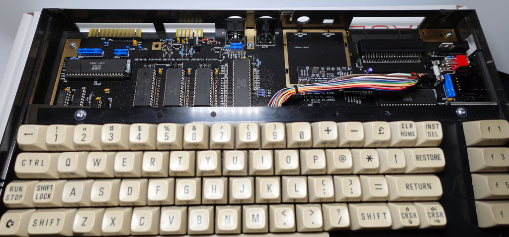
The keyboard is lent from an original 250466 system until new keycaps are finally available.
The case is a reproduction created with the original machines and sold by iComp.
All files related to this project including the DipTrace schematic/layout files can be found in the BitBucket
repository
https://bitbucket.org/fade0ff/c64-250466/
This is a spare time project I did without any commercial interest.
Everything is released under the Creative
Commons CC-BY license.

In a nutshell this means that you can do share, modify and use
everything released under this license even for commercial projects.
You just need to give me appropriate credit, indicate what changes you
made and agree not to try to force a more restrictive license on my
work.
See the CC BY license for details.