Since the device is meant for automotive development, chances are that sooner or later one of the outputs will be connected to either ground or battery voltage (usually 13.5V, but up to 20V possible).
Short circuit to ground is not an issue due to the output impedance of ~50Ohm.
Short circuit to battery is not much of an issue for the output driver
(TC4469cpd) as it is designed to support supply voltage up to 18V, handle
peak currents of 1.2A and a continuous output current of 300mA per output
or 500mA for the package.
I.e. if somebody connects to the output to 13.5V while the internal
push-pull stage is switched to GND, the output impedance (no acting
as input impedance) of 50Ohm will limit the current to 13.5V/50Ohm =
0.27A.
For higher voltages of course the current becomes too high
for the driver and also for the output resistor.
A typical protection approach for overvoltage protection is to add a
clamping (suppressor) diode that has no influence (apart from a small
capacity) as long as certain voltage threshold is not exceeded, but
behaves like a short circuit when the voltage rises above this threshold.
A suppressor diode with good availability is the 1N5908 "TRANSIL" (ST). It
defines a "REVERSE STAND OFF VOLTAGE" of 5V. However when looking at
the datasheet you'll see that this doesn't mean its actual threshold is
5V.
Indeed the breakdown voltage is 6V at 1mA, but the clamping voltage rises
with the current.
With the given resistance of ~50Ohm, the actual clamping voltage when
connecting 20V was measured to be ~6.7V which is safe enough to protect
the output driver, yet of course the (reverse) current through the
resistor would destroy it sooner or later.
E.g. when connecting 30V to the output and taking into account a clamping voltage of
~7V and a resistance of ~50Ohm, the remaining voltage difference of 23V means that about 460mA
((30V-7V)/50Ohm) will be flowing through the suppressor diode and thus
through the resistor.
Since P = I2R , for 460mA and 50Ohm, this would result in a power
of 10.58W, effectively destroying any normal resistor. Therefore a
polyfuse is added in series with the output resistor. It is designed to
limit currents by becoming high ohmic above a certain current threshold.
The good thing is that it's self resetting, so no need to exchange the
fuse after it tripped. Bad thing is that polyfuses are pretty slow.
However the larger the voltage and the current, the faster the fuse will trip.
Besides, a 2W resistor was chosen as output resistor which can tolerate
around 10W for 10s, so there's a good chance that the polyfuse will trip
before the resistor is damaged.
Unfortunately, there is one more case to consider, namely a short circuit
to battery while the push-pull driver is switched to "high" (5V). In this
case, the overvoltage is connected to the 5V net via the highside
transistor of the push-pull driver.
Since the suppressor/clamping diode will limit the voltage to around 7V,
this means that everything connected to the 5V net will be supplied with
7V in short circuit condition while the shortened output is switched high.
So e.g. the MAX202, the CAN transceiver and the LCD display will be
supplied with 7V instead of 5V. Even if they survive this, their outputs
connected to microcontroller inputs (RX for UART/CAN and 4 LCD data lines)
will also have 7V.
As the inputs of the LPC1768 are only 5V tolerant with a maximum allowed
voltage of 6V, this could destroy the microcontroller.
I thought about disabling the TC4469 in overvoltage condition but this
created an oscillation as the overvoltage condition was removed when
disabling, thus enabling again etc.
Instead I decided to use a P-FET that disconnects the output if the output
voltage gets too high.
To detect the overvoltage, a shunt regulator TL431 is used. It is more
accurate than a Zener diode, has less temperature dependency and can be configured for a specific voltage.
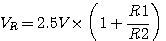
With R1 = 20kOhm and R2 = 22kOhm this yields 4.773V.
This reference voltage is used to switch a PNP transistor to GND in case the voltage at the output exceeds ~5.1V (note: BJT transistors usually need ≥0.4V difference between emitter and base to switch through) which again switches a P-FET.
In inactive state, the output voltage doesn't exceed 5.1V, so the PNP transistor is off (high ohmic). Therefore the gate of the P-FET is pulled to ground, resulting in a VGS of -5V which means the P-FET is fully switched through and has only a small resistance of ~0.6Ohm:

Now the output is connected to 6.9V, which are directly connected to the
emitter of the PNP transistor. As the base's voltage is only 4.77V, it will
switch through.
Thus the 6.9V of the output are connected to the base of the P-FET. VGS
becomes ~0V and the FET's channel becomes inactive (high ohmic).
Effectively, only the FET's body diode remains active, so current can only
flow from the driver to the output while reverse current is blocked.

With this circuit in place, the voltage left of the P-FET (drain side) can
never exceed 5.1V and as soon as the P-FET becomes inactive, it will be
exactly 5V.
When placing this circuit between the supply of the output driver (TC4469)
and the normal 5V net, one circuit can protect all outputs.
The driver's supply voltage will be raised to ~7V in case of a short circuit
to battery with enabled highside, but this won't damage the driver.
A small drawback is that all other outputs will be use a high state voltage
of 7V as well during this short circuit condition, but this should be
tolerable.